1 / 5
| Model NO. | HMLY-DB-005 |
| Laser Visibility | Visible |
| Applicable Material | Metal / Semiconductor |
| Cooling System | Air Cooling / Water Cooling Options |
| Laser Wave | 355nm / 532nm / 1064nm |
| Laser Power | 4W / 7W / 10W / 15W / 25W |
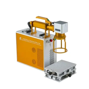
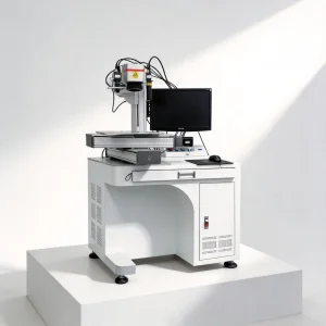
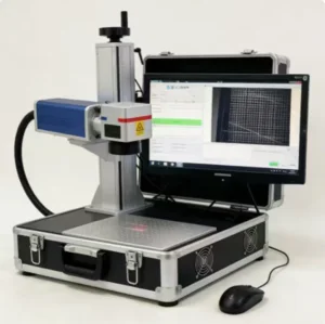
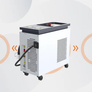
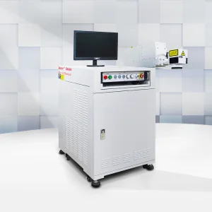
| Type | Semiconductor Laser Marking Machine |
| Sub-Micron Accuracy | Precision Alignment for <10μm Marks |
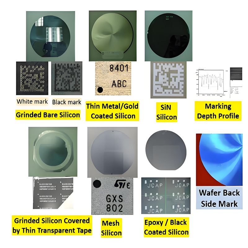
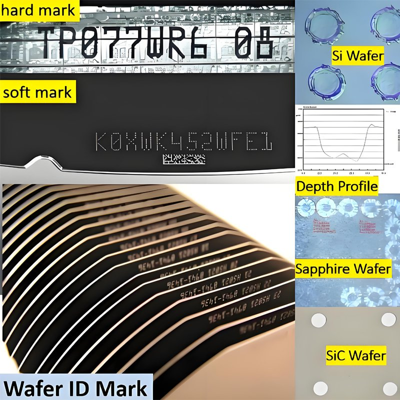
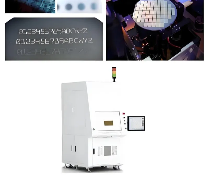
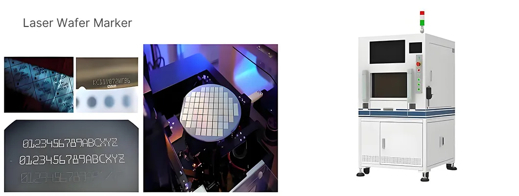
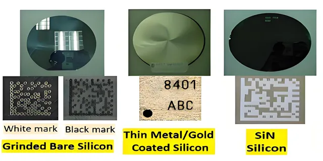
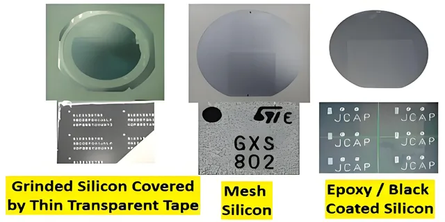
| Material Versatility | Si, GaAs, Sic, and Compound Wafers |
| Traceability | Semi T7 & Secs/Gem Standards |
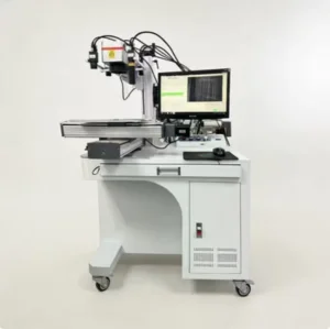
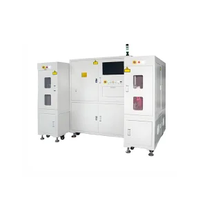
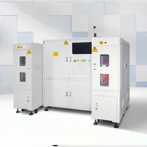
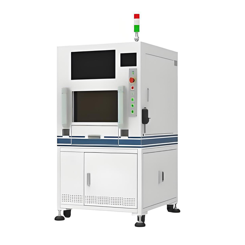
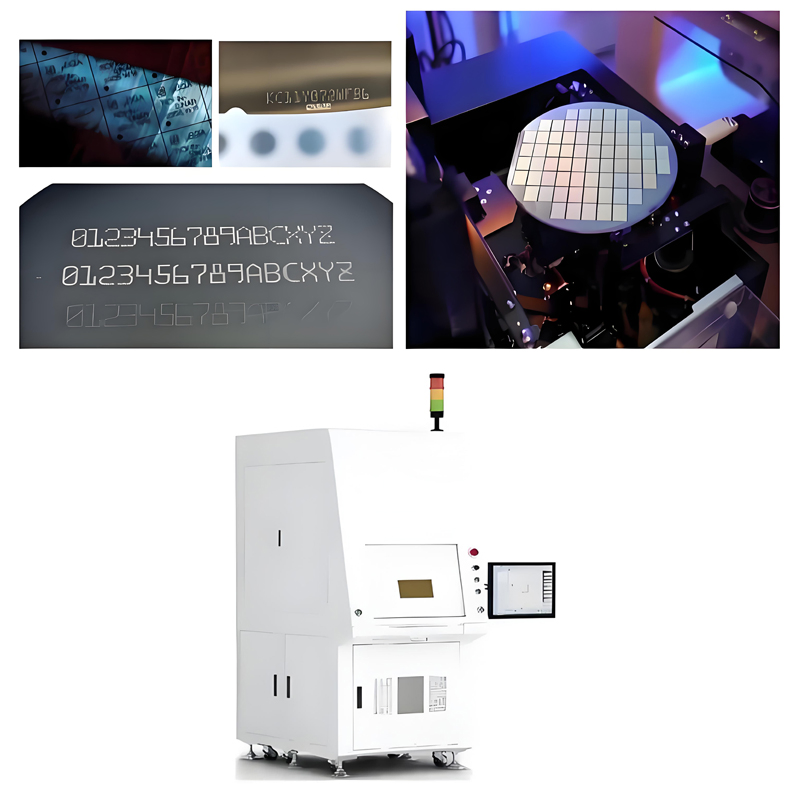
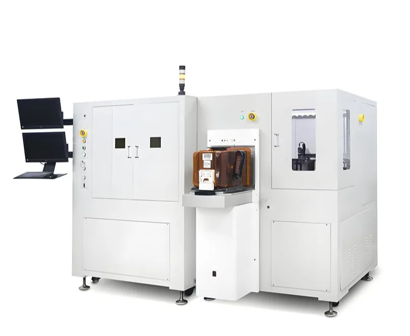
The Wafer Marking Machine is a high-precision, automated system designed for the laser marking of semiconductor wafers with 8-12-inch compatibility. It integrates robotic handling, automatic calibration, and advanced laser marking to ensure efficient and clean processing. The machine supports SECS/GEM communication and can be customized for various marking patterns, including barcodes (SEMI T1) and QR codes, while maintaining ISO Class 2 cleanliness.
| Parameter | Details |
|---|---|
| Laser Wavelength | 532nm |
| Cooling Method | Water Cooling |
| Control System | Galvanometer + Control Card (Windows 7/10) |
| Supported Formats | DXF, PLT |
| Power Supply | Single-Phase 220V, 4KW |
| Optional Features | QR Code (DM), Custom Marking Designs |
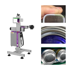
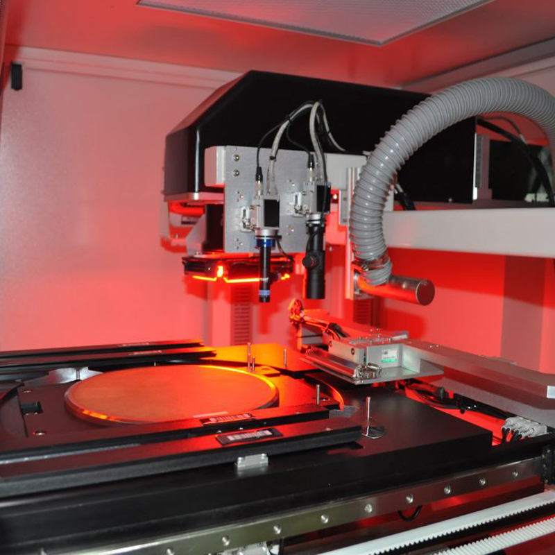
Equipped with 532nm laser for clear and durable wafer markings.
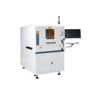
Dual-arm robotic system with ±0.1mm repeatability for loading/unloading.
3-second center and angle detection for accurate positioning.
Temp: 20-25°C; Humidity: 35-60%; Power: 220VAC, 50Hz.
Unique Wafer Marking (UWM) for 8-12 inch wafers; Lot & Batch Tracking.
Laser Marking for Mini/Micro-LEDs on GaN, SiC, and sapphire wafers.
SiC & GaN Power Devices for EV inverters and industrial modules.
Identifies MEMS wafers before dicing; glass-frit sealed medical applications.